Logo specs-groupDetail

Mimea

The base package provides all the functions for fundamental SPM applications, in particular STM and contact mode AFM. From signal conditioning and AD/DA conversion to FPGA and real-time signal processing and graphical user-interface, the Nanonis Base Package provides a complete framework that can be adapted and extended with a wide range of add-on modules.

RELATED PRODUCTS

APPLICATION NOTES

Piezoelectric Quartz Tuning Forks for Scanning Probe Microscopy
In this paper the application of piezoelectric quartz tuning forks in dynamic force microscopy is described. For the introduction we give a historical overview and a comparison with traditional cantilevers. In the second section the theories for tuning forks as oscillators for the dynamic force detection are introduced and in the third section the experimental implementation is described.
download PDF
OC4-Station and VEECO EnviroScope - Advanced Vacuum Measurements
Veeco EnviroScope combines a hermetically sealed sample chamber with scanning microscopy. Due to the relative high Q factor of the cantilevers in vacuum this instrument can be operated with an external PLL for advanced combined measurements, i.e. nc-AFM, MFM, EFM…
download PDF
Single Pass Kelvin Probe Measurement Technique in Air with Dual-OC4
The Kelvin probe technique is increasingly gaining importance in AFM measurements since it gives access not only to the topography but also to chemical information of the tip and sample. It is an extremely sensitive analytical method to detect changes in contact potential difference between different materials or chemical elements on the surface.
download PDF
Compensating for CPD in NC-AFM: AM-KPFM in UHV using Dual-OC4
Single pass Kelvin probe imaging (KPFM) gives information on the electronic structure of materials by measuring contact potential difference (CPD) while simultaneously acquiring topography. Under vacuum condition the Q factor is higher than in air, leading to higher resolution for both Kelvin and topography images.
download PDF
Far-Field Fibered Interference Scanning Optical Microscopy (iSOM) - Imaging Living Cells
In the field of biology, the scanning techniques in air or liquid environments are nowadays intensively used. AFM, STM, SNOM are relatively fast imaging methods allowing sub-µ resolution, in contrast with conventional optics allowing for fast and noncontact imaging, but suffering from lack of resolution according to Rayleigh criterion.
download PDF
Modulation of Contact Resonances: Use of PLL in Contact Mode AFM
Friction force microscopy (FFM) is a useful technique capable of characterizing material mechanical properties, such as elastic module, adhesion, and friction down to atomic scale. When combining static lateral force measurements with dynamic measurements of contact resonance frequencies the sensitivity is improved, i.e. subsurface defects are easier to detect than in conventional quasi static FFM.
download PDF
Friction Force Microscopy
Friction force microscopy (FFM) is a powerful tool which allows us to study the origin of friction in single asperity contacts. The observation of atomic stick-slip and its variation with load, during the sliding of tip against another solid surface provides detailed information about the dissipation mechanisms. Statistical averaging of repeated measurements with good control over experimental parameters is of crucial importance for reliable FFM measurements.
download PDF
Feenstra Type of Spectroscopy: Making use of the Programming Interface
Spectroscopic measurements in STM are an important tool for the investigation of the electronic states at surfaces. When combined with the variable tip-sample separation technique this type of spectroscopy leads to high dynamic range, 5 to 6 orders of magnitude, in the measured current and conductance even on the semiconductor surfaces with low surface state density.
download PDF
Improved Atomic Scale Contrast via Bimodal DFM: Dual OC4
Frequency-modulation atomic force microscopy (FM-AFM) is an efficient and already widely spread technique to obtain atomically resolved images of insulating or metallic surfaces. Typically, FM-AFM is based on scanning a sharp tip of a macroscopic cantilever over the surface, where the tip-surface distance is usually controlled by the frequency shit (f1) of the first normal resonant mode (f1) of the cantilever. The atomic-scale contrast arises from short range forces; e.g. covalent or ionic bonds, thus the detection sensitivity of the FM-AFMcan be improved by using small tip oscillation amplitudes comparable to the decay length of the short-range forces, ~ 0.1 nm. A lot of efforts are put in this direction in the FM-AFMfield, mainly based on the excitation of a tuning fork sensor or higher flexural modes of cantilevers characterized by largerstiffness.
download PDF
Atom Tracking used for Reproducible Force Spectroscopy
Force spectroscopy in dynamic force microscopy at room temperature is a challenging feat due to the unavoidable thermal drift. Especially in three dimensional force spectroscopy, even a tiny drift of around 10 pm over the measurement will result in a crucial error.
download PDF
Automated Amplitude Calibration in non-contract AFM Mode
Calibration procedures are always very important for correct quantitative measurements in SPM. In the absence of an interferometer, acquiring an accurate calibration using nc-AFM is complicated. The routine also has to be repeated multiple times for an accurate determination of the amplitude calibration factor which requires a non-negligible amount of time.
download PDF
Mapping the Orbital Structure of Impurity Bound States in a Superconductor
Superconductivity is a low-temperature phenomenon caused by the pairing of electrons via interactions me-diated by the environment. A signature of supercon-ductivity is that no single electron can be injected at low energies because the only possible states are the ones corresponding to pairs of electrons. Hence, an absolute gap in the density of states (DOS) is a finger-print of conventional superconductors. In s-wave su-perconductors such as lead the paired electrons (i.e. the Cooper pairs) have opposite spin. An external magnetic field forces the electron spins to align, there-by breaking the pairing and destroying superconductivity.
download PDF
Drift-Corrected 3D Dynamic Force Spectroscopy at Room Temperature
The ability to collect 3D dynamic force spectroscopy (DFS) data opens the door to valuable and more complete information of the interaction forces at the atomic scale. True site-specific atomic scale interaction forces and potential energies were accessible before mainly at low temperatures due to the absence of instrumentation-induced artifacts.
download PDF
Realization of a Tunable Artificial Atom at a Supercritically Charged Vacancy in Graphene
This is the first observation ever of a stable and tuneable charged vacancy in graphene and could allow researchers to fabricate artificial atom arrays for performing the electronic equivalent of optical operations.
download PDF
Automated Switching Between Non-Contact and Contact Modes of AFM
The study of plasticity by means of atomic force microscopy (AFM) is a fascinating experiment, as it is possible to observe the nucleation of single dislocations directly in the indentation force curve and image the resulting deformed surface structure with high resolution.
download PDF
Non-Contact Atomic Resolution in Liquid Using Nanonis OC4
AFM imaging in liquid is often challenging due to poor quality factor of the cantilever and high environmental noise. With these challenges in mind, we constructed a beam-deflection AFM designed for imaging in various environments [1, 2]. Since we wanted to operate our AFM in frequency modulation mode, we combined the Nanonis OC4 (used as a PLL) together with the Asylum MFP3D controller and were able to obtain true atomic-resolution in liquid (right image).
download PDF
Optimizing PLL Feedback Parameters: Nanonis perfectPLL
Setting up a phase-locked loop (PLL) for use in non-contact applications is difficult. Four free feedback parameters for amplitude and phase control and two additional free parameters for the z-feedback leave a lot of room for incorrect settings and unwanted tip-crashes. Therefore we wanted to find a simple and reliable way to set up our PLL.
download PDF
Ultra-Low Current STM at 100fA
Scanning at ever lower currents is an ongoing effort in the STM community. In a test run at the University of Lille, the Nanonis control system was put to test with an Omicron-1 STM to measure atomic resolution images on a Si-111 sample.
download PDF
22-bit on all Ouput Channels: Nanonis hrDAC
In digital SPM control system the resolution of the digital-analog converters has always been a limiting factor, both in achieving atomic resolution and in spectroscopy applications. The newly developed hrDAC™ not only overcomes these limitations, but compared to the usual offset/gain approach, also has a series of other advantages.
download PDF
Integrating External Equipment - User Chanenels in the Nanonis SPM controller
We use the Nanonis SPM Control System and Oscillation Controller to operate our tuning fork-based JEOL microscope. The z-feedback runs on the frequency shift of the tuning fork. To make local capacitance measurements we attached a separately contacted metal tip to one prong of the tuning fork. In our effort to map local charge defects in Hf-based high-k gate films we had to integrate the signals from two ex-ternal lock-in detectors with the data acquisition of the control system.
download PDF
Doing Electrochemistry with an SPM tip: EC-SPM
Electrochemical SPM (EC-SPM) in liquid electrolytes provides an addi-tional level of experimental control for in-situ studies of surfaces and redox active adsorbates. Independent control of the tip and surface electrode potentials enables atomic resolution imaging and spectros-copy of electrochemical surface processes. This method allows for real-time analysis of electrochemical processes occurring at the electrolyte-surface interface as compared to ex-situ methods and has proven to be an invaluable experimental tool in the fields of electrochemistry and surface science.
download PDF
Single-Scan Kelvin Probe Technique in Air with Dual Oscillation Controller
In atomic force microscopy electrostatic forces are usually not discriminated against van-der-Waals forces. Attractive electrostatic forces cause the distance controller to retract the tip from the surface, resulting in erroneous height information in the topography image. Together with Nanonis we developed a novel solution to this longstanding problem.
download PDF
Atom Manipulation with Nanonis SPM Controller
Atom manipulation often attracts the interest of researchers, not only for observing artificial patterns on the surface, but also since it allows preparing ideal “samples” on surfaces, designed for a specific measurement. At the same time, however, it often requires a complete custom made scanning probe controller. Although the first systematic atom manipulation was demonstrated in 1990s, it is still challenging for mostresearchers. This application notes shows how the fully-digital Nanonis SPM controller with its LabVIEW Programming Interface can significantly reduce the technical challenges and simplify the manipulation process.
download PDF
Needle Sensor Operation in non-contact AFM Mode
Needle sensors are becoming increasingly popular to measure the tunneling current while not depending on the current for the distance feedback. A resonance frequency of 1 MHz insures a fast response of the sensor while interacting with the surface, but it requires a highly accurate Phase Locked Loop (PLL) to perform non-contact AFM measurements, especially with low frequency shift set points.
download PDF
Femtogram Resolution for In-Situ Monitoring of FIB and E-Beam Induced Milling
The optimization of focused ion and electron beam induced processes for the reliable fabrication of micro- and nanodevices has been of increasing importance. For this a further understanding of the basic physics underlying the process is necessary. In-situ process monitoring is an efficient way to move forward in this field.
download PDF
Trapped 2D free e- Gas of Cu(111) withinRegular Array of QDs: STS study
Two dimensional quantum confinements at surfaces have always been a challenge for the scientists, mainly because of the difficulties to produce regular nanopatterns that can trap electronic states. One possibility of analyzing such structures is Scanning tunneling Microscopy (STM) and Spectroscopy (STS) at low temperature.
download PDF
Supramolecular Rotary Device
For years a lot of efforts have been put on designing organic molecules whose properties can be exploited for building up artifi cial molecular devices. Together with our partners from the University of Basel and the ETH Zurich we created a specially functionalized molecule that on a Cu(111) surface does not only form a nanoporous network, but also have the right size to be nested on top of the pores.
download PDF
Controlling QPlus small Amplitudes with Nanonis Setup
A growing number of users are opting for a modified setup of their STM combining a standard instrument with a QPlus Sensor to do non-contact AFM. QPlus sensors can be easily integrated with the existing STM head since they are based on oscillations of quartz tuning forks. The detection of such oscillations is done electrically and no additional laser system is required. When combined with low temperature this technique leads to a large spectrum of applications.
download PDF
Exploring Nanoelectromechanic of Ferroelectrics: PFM with Dual-OC4
Piezoresponse Force Microscopy (PFM) is now the primary technique for imaging, spectroscopy, and domain patterning in ferroelectric materials. Piezoresponse (PR) studies of ferroelectric materials has started in the beginning of 90s [1], and today undergo exponential growth due to rapidly emerging applications of ferroelectric and multiferroic materials for nonvolatile memories and data storage [2, 3]. These applications have stimulated extensive efforts toward understanding the mechanisms for polarization reversal in ferroelectrics on the nanometer scale.
download PDF
High-Resolution Imaging and Spectroscopy of Water on NaCl(001) Surface
The interaction of water with the surfaces of solid ma-terials is ubiquitous. Many remarkable physical and chemical properties of water/solid interfaces are gov-erned by H-bonding interaction between water mole-cules. As a result, the atomic-scale description of H-bonding structure and dynamics is one of the most important fundamental issues in water science. Ideally, attacking this problem requires the ability to access the internal degrees of freedom of water molecules, which remains a great challenge due to the light mass and small size of hydrogen.
download PDF

PUBLICATIONS

  1. (2021) Multiband charge density wave exposed in a transition metal dichalcogenide

    In the presence of multiple bands, well-known electronic instabilities may acquire new complexity. While multiband superconductivity is the subject of extensive studies, the possibility of multiband charge density waves (CDWs) has been largely ignored so far. Here, combining energy dependent scanning tunnelling microscopy (STM) topography with a simple model of the charge modulations and a self-consistent calculation of the CDW gap, we find evidence for a multiband CDW in 2H-NbSe2. This CDW not only involves the opening of a gap on the inner band around the K-point, but also on the outer band. This leads to spatially out-of-phase charge modulations from electrons on these two bands, which we detect through a characteristic energy dependence of the CDW contrast in STM images.


    A. Pásztor, A. Scarfato, M. Spera, F. Flicker, C. Barreteau, E. Giannini, J. van Wezel, and C. Renner
    Nat Commun 12, 6037 (2021)
    Read more
  2. (2010) Imaging Coulomb islands in a quantum Hall interferometer

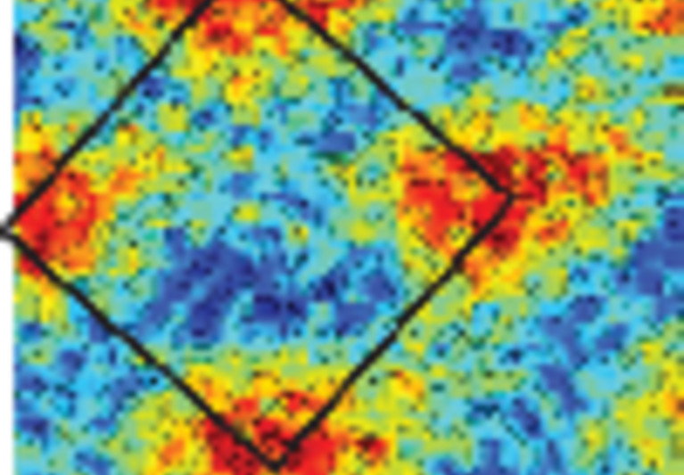
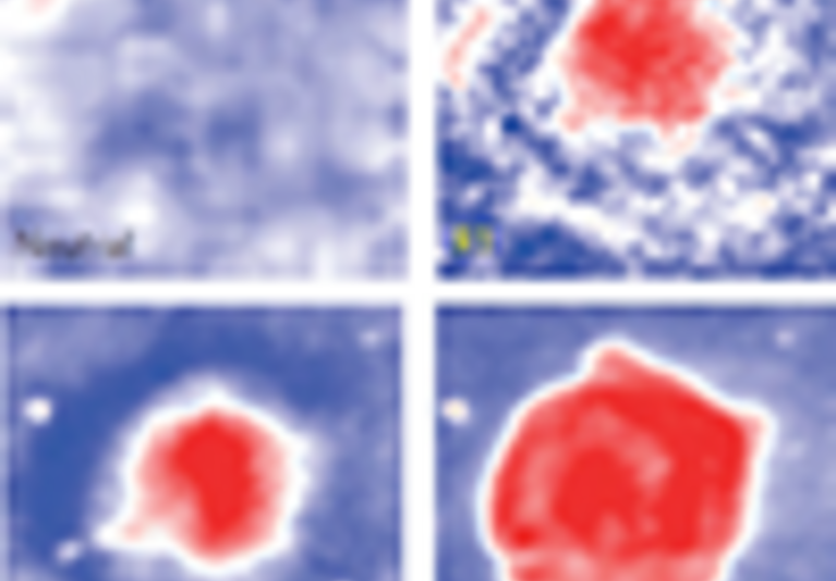
    In the quantum Hall regime, near integer filling factors, electrons should only be transmitted through spatially separated edge states. However, in mesoscopic systems, electronic transmission turns out to be more complex, giving rise to a large spectrum of magnetoresistance oscillations. To explain these observations, recent models put forward the theory that, as edge states come close to each other, electrons can hop between counterpropagating edge channels, or tunnel through Coulomb islands. Here, we use scanning gate microscopy to demonstrate the presence of QH Coulomb islands, and reveal the spatial structure of transport inside a QH interferometer. Locations of electron islands are found by modulating the tunnelling between edge states and confined electron orbits. Tuning the magnetic field, we unveil a continuous evolution of active electron islands. This allows to decrypt the complexity of high-magnetic-field magnetoresistance oscillations, and opens the way to further local-scale manipulations of QH localized states.


    B. Hackens, F. Martins, S. Faniel, C.A. Dutu, H. Sellier, S. Huant, M. Pala, L. Desplanque, X. Wallart, V. Bayot
    Nature Communications volume 1, Article number: 39
    Read more
  3. (2010) Near-field scanning optical microscopy using polymethylmethacrylate optical fiber probes

    We report the first use of polymethylmethacrylate (PMMA) optical fiber-made probes for scanning near-field optical microscopy (SNOM). The sharp tips were prepared by chemical etching of the fibers in ethyl acetate, and the probes were prepared by proper gluing of sharpened fibers onto the tuning fork in the conditions of the double resonance (working frequency of a tuning fork coincides with the resonance frequency of dithering of the free-standing part of the fiber) reported earlier for the case of glass fibers. Quality factors of the probes in the range 2000–6000 were obtained, which enables the realization of an excellent topographical resolution including state-of-art imaging of single DNA molecules. Near-field optical performance of the microscope is illustrated by the Photon Scanning Tunneling Microscope images of fluorescent beads with a diameter of 100 nm. The preparation of these plastic fiber probes proved to be easy, needs no hazardous material and/or procedures, and typical lifetime of a probe essentially exceeds that characteristic for the glass fiber probe.


    H.Chibani, K.Dukenbayev, M.Mensi, S. K. Sekatskii, G.Dietler
    Ultramicroscopy Vol. 110 (3), pp 211-215
    Read more
  4. (2010) Scanning near-field optical microscopy-based study of local dynamics of receptor-ligand interactions at the single molecule level

    A scanning near-field optical microscope (SNOM)—based modification of the method to study the dynamics of single molecule receptor—ligand interactions exploiting the fluorescence imaging by total internal reflection fluorescence microscopy is introduced. The main advantage of this approach consists in the possibility to study the single molecule interaction dynamics with a subwavelength spatial resolution and a submillisecond time resolution. Additionally, due to the much smaller irradiation area and some other technical features, such a modification enables to enlarge the scope of the receptor—ligand pairs to be investigated and to improve the temporal resolution. We briefly discuss corresponding experimental set up with a special accent on the SNOM operation in liquid and present some preliminary results of related investigations.


    M. Mensi, K. Dukenbayev, S. K. Sekatskii, G. Dietler
    Laser Physikcs, Vol. 20 (1), pp 78-84
    Read more
  5. (2010) Morphology Mapping of Phase-Separated Polymer Films Using Nanothermal Analysis

    Polymers films are attractive, in part, because their physical properties can be tuned by blending polymer with complementary characteristics. However, blending is typically challenging because most polymers will undergo phase separation, resulting in unpredictable behavior. Here, we introduce band excitation nanothermal analysis (BE-NanoTA) as a nondestructive AFM-based technique for mapping the near surface, thermal properties of polymeric coatings. BE-NanoTA was used to investigate phase separation and domain growth in poly(styrene-ran-acrylonitrile):poly(methyl methacrylate) SAN:PMMA films. The size and shape of PMMA-rich domains are consistent with prior measurements on the same system using a destructive method, namely UV-ozone etching of PMMA followed by topography mapping using standard AFM. Moreover, new insights into the mechanism of phase separation were uncovered including the observation of SAN- and PMMA-rich channels near the surface at early times as well as small SAN-rich domains trapped within large PMMA domains during intermediate times. Because it is nondestructive, BE-NanoTA can be used to explore in situ phase evolution in soft matter systems (e.g., polymer nanocomposites) which do not lend themselves to the UV-ozone etching method.


    M. P. Nikiforov, S. Gam, S. Jesse, R. J. Composto, S. V. Kalinin
    Macromolecules, 43 (16), pp 6724–6730
    Read more
  6. (2010) Time-resolved scanning tunnelling microscopy for molecular science

    Time-resolved scanning tunnelling microscopy (STM) and its application in molecular science are reviewed. STM can image individual atoms and molecules and thus is able to observe the results of molecular processes such as diffusion, desorption, configuration switching, bond-breaking and chemistry, on the atomic scale. This review will introduce time-resolved STM, its experimental limitations and implementations with particular emphasis on thermally activated and tunnelling current induced molecular processes. It will briefly examine the push towards ultrafast imaging. In general, results achieved by time-resolved STM demonstrate the necessity of both space and time resolution for fully characterizing molecular processes on the atomic scale.


    P. A. Sloan
    J. Phys.: Condens Matter 22, 264001
    Read more
  7. (2010) A low noise all-fiber interferometer for high resolution frequency modulated atomic force microscopy imaging in liquids

    We have developed a low noise all-fiber interferometer for use as the deflection sensor in liquid environment frequency modulated atomic force microscopy (FM-AFM). A detailed description and rationale for the choice of the critical components are provided along with the design of a simple alignment assembly. The optimization of the deflection sensor toward achieving the highest possible sensitivity and lowest deflection noise density is discussed in the context of an ideal interference cavity. Based on the provided analysis we have achieved deflection noise densities of 2 fm/√ Hz on commercially available cantilevers in both ambient and liquid environments. The low noise interferometer works without the need for differential detection, special focusing lenses, or polarization sensitive optics, dramatically simplifying measurements. True atomic resolution imaging of muscovite mica by FM-AFM in water is demonstrated using the developed deflection sensor.


    H. I. Rasool, P. R. Wilkinson, A. Z. Stieg, J. K. Gimzewski
    Review of Scientific Instruments 81, 023703
    Read more
  8. (2010) NaCl islands decorated with 2D or 3D 3,4,9,10-perylene-tetracarboxylic-dianhydride nanostructures

    The formation of PTCDA (3,4,9,10-perylene-tetracarboxylic-dianhydride) nanostrutures on Au(1 1 1)- (22 x √ 3) covered with NaCl islands has been studied using scanning tunneling microscopy (STM). Atomically resolved STM images show that NaCl grows as (1 0 0)-terminated layers on Au(1 1 1)- (22 x √ 3) . Local atomic hexagonal packing has also been observed in the NaCl(1 0 0) layer. At submonolayer NaCl coverage, PTCDA forms two-dimensional islands on the Au(1 1 1) surface and nucleate preferentially at the NaCl island step edges. When the Au surface is fully covered with NaCl layers, PTCDA molecules form three-dimensional molecular clusters decorating the step edges of NaCl layers.


    X. Sun, F. Silly
    Appl. Surf. Sci. Vol. 256 (7), 2228
    Read more
  9. (2010) Experimental and theoretical analysis of H-bonded supramolecular assemblies of PTCDA molecules

    Using a systematic method based on considering all possible hydrogen bond connections between molecules and subsequent density-functional theory (DFT) calculations, we investigated planar superstructures that the perylene-3,4,9,10-tetracarboxylic-3,4,9,10-dianhydride (PTCDA) molecules can form in one and two dimensions. Structures studied are mostly based on two molecule unit cells and all assemble in flat periodic arrays. We show that 42 different monolayer structures are possible, which can be split into eight families of distinct structures. A single representative of every family was selected and relaxed using DFT. We find square, herringbone and brick wall phases (among others) which were already observed on various substrates. Using scanning tunneling microscopy in ultrahigh vacuum, we also observed herringbone and square phases after sublimation of PTCDA molecules on the Au(111) surface at room temperature, the square phase being observed for the first time on this substrate. The square phase appears as a thin stripe separating two herringbone domains and provides a perfect structural matching for them. A similar structural formation serving as a domain wall between two other phases has been recently reported on the same surface formed by melamine molecules [F. Silly et al., J. Phys. Chem. C 112, 11476 (2008)]. Our theoretical analysis helps to account for these and other observed complex structures.


    M. Mura, X. Sun, F. Silly, H. T. Jonkman, G. A. D. Briggs, M. R. Castell, L. N. Kantorovich
    Phys. Rev. B 81, 195412
    Read more
  10. (2010) Tailoring two-dimensional PTCDA–melamine self-assembled architectures at room temperature by tuning molecular ratio

    Engineering and tuning multi-component supramolecular self-assemblies on surfaces is one of the challenges of nanotechnology. We use scanning tunneling microscopy to investigate the influence of molecular ratio on the self-assembly of PTCDA–melamine structures on Au(111)-(22 x √ 3). Our observations reveal that three different chiral supramolecular networks having a PTCDA:melamine ratio of 3:2, 1:2, 1:4 can be selectively created by tuning the ratio of molecules deposited on the surface. The 1:2 ratio network having melamine in excess has been observed previously but the 1:4 network has not yet been reported. In comparison, the multi-component 3:2 network having PTCDA in excess is a completely new structure.


    X. Sun, H. T. Jonkman, F. Silly
    Nanotechnology, 21(16):165602
    Read more
  11. (2010) Atomic force microscopy imaging using a tip-on-chip: Opening the door to integrated near field nanotools

    We describe in detail how atomic force microscopy (AFM) images can be routinely achieved with macroscopic silicon-based chips integrating mesoscopic tips, paving the way for the development of new near field devices combining AFM imaging with any kind of functionality integrated on a chip. The chips have been glued at the end of the free prong of 100 kHz quartz tuning forks mounted in Qplus configuration. Numerical simulations by modal analysis have been carried out to clarify the nature of the vibration modes observed in the experimental spectra. It is shown that two low frequency modes can be used to drive the system and scan the surface with a great stability in amplitude modulation as well as in frequency modulation AFM under ultrahigh vacuum. The AFM capabilities are demonstrated through a series of examples including phase and dissipation contrast imaging, force spectroscopy measurements, and investigations of soft samples in weak interaction with the substrate. The lateral resolution with the tips grown by focused ion beam deposition already matches the one achieved in standard amplitude modulation mode AFM experiments.


    J. Hayton, J. Polesel-Maris, R. Demadrille, M. Brun, F. Thoyer, C. Lubin, J. Cousty, B. Grévin
    Review of Scientific Instruments 81, 093707
    Read more
  12. (2010) Dynamic behavior of amplitude detection Kelvin force microscopy in ultrahigh vacuum

    The acquisition rate of all scanning probe imaging techniques with feedback control is limited by the dynamic response of the control loops. Performance criteria are the control loop bandwidth and the output signal noise power spectral density. Depending on the acceptable noise level, it may be necessary to reduce the sampling frequency below the bandwidth of the control loop. In this work, the frequency response of a vacuum Kelvin force microscope with amplitude detection (AM-KFM) using a digital signal processing (DSP) controller is characterized and optimized. Then, the main noise source and its impact on the output signal is identified. A discussion follows on how the system design can be optimized with respect to output noise. Furthermore, the interaction between Kelvin and distance control loop is studied, confirming the beneficial effect of KFM on topography artefact reduction in the frequency domain. The experimental procedure described here can be generalized to other systems and allows to locate the performance limitations.


    H.Diesinger, D.Deresmes, J.-P. Nys, T.Mélin
    Ultramicroscopy Volume 110, Issue 2
    Read more
  13. (2010) Local surface photovoltage spectroscopy of Cu-phthalocyanine clusters on different substrates

    Cu-phthalocyanine (CuPc) serves as a very efficient absorber molecule in organic solar cell devices. The authors have applied spatially resolved surface photovoltage spectroscopy in a Kelvin probe force microscope to investigate the absorption and exciton separation of CuPc molecules on Si(100) and ITO substrates. A positive surface photovoltage was observed for illumination energies above ~ 1.5 eV, indicating absorption of the light in the CuPc molecules and subsequent separation of holes into the substrate.


    S. Sadewasser, M. Ch. Lux-Steiner
    Journal of Vacuum Science & Technology B 28, C4D29
    Read more
  14. (2010) Mapping charge transfers between quantum levels using noncontact atomic force microscopy

    We demonstrate the possibility to map nanoscale charge transfers between quantum electronic levels at room temperature, using noncontact atomic force microscopy and Kelvin force microscopy in a regime of weak electromechanical coupling. A two-level system is studied, consisting of degenerately doped silicon nanocrystals on silicon substrates, with size in the 2–50 nm range, in which the energy spacing is tuned by the nanocrystal quantum confinement over a ≈1 eV range. The nanocrystal ionization is found to follow an energy compensation mechanism driven by quantum confinement, in quantitative agreement with parametrized tight-binding calculations of its band structure.


    Ł. Borowik, K. Kusiaku, D. Deresmes, D. Théron, H. Diesinger, T. Mélin, T. Nguyen-Tran, P. Roca i Cabarrocas
    Phys. Rev. B 82, 073302
    Read more
  15. (2011) Flipping Behavior of a Porphyrin Derivative Molecule on a Au(111) Reconstructed Surface

    Porphyrin derivative molecules (MP-tBPP) on a Au(111) reconstructed surface have been investigated using scanning tunneling microscopy. The molecules were found to adsorb with two kinds of orientation at the elbow positions of the reconstructed surface. One orientation had the two di-tert-butylphenyl groups of a molecule aligning along a row of elbow positions, and the other was the same alignment rotated approximately 60°. Flipping behaviors from one orientation to the other were observed in successively obtained scanning tunneling microscopy images. The activation energy for the flipping behaviors was estimated to be approximately 60 meV from the flipping rates. The difference in the molecular populations with each of the orientations represents the potential energy of the adsorbed molecules having asymmetric double minima corresponding to the two orientations. The difference between the potential energies of the molecules in these orientations was approximately 12 meV, which was calculated from the ratio between the populations in the orientations and from the difference in the flipping rates.


    H. Suzuki, H. Yoshida, H. Sakaue, T. Takahagi, S. Tanaka, T. Kamikado, A. Otomo
    J. Phys. Chem. C, 115 (25), pp 12414–12418
    Read more
  16. (2011) Force gradient sensitive detection in lift-mode Kelvin probe force microscopy

    We demonstrate frequency modulation Kelvin probe force microscopy operated in lift-mode under ambient conditions. Frequency modulation detection is sensitive to force gradients rather than forces as in the commonly used amplitude modulation technique. As a result there is less influence from electric fields originating from the tip's cone and cantilever, and the recorded surface potential does not suffer from the large lateral averaging observed in amplitude modulated Kelvin probe force microscopy. The frequency modulation technique further shows a reduced dependence on the lift-height and the frequency shift can be used to map the second order derivative of the tip–sample capacitance which gives high resolution material contrast of dielectric sample properties. The sequential nature of the lift-mode technique overcomes various problems of single-scan techniques, where crosstalk between the Kelvin probe and topography feedbacks often impair the correct interpretation of the recorded data in terms of quantitative electric surface potentials.


    D. Ziegler, A. Stemmer
    Nanotechnology 22, 075501
    Read more
  17. (2011) Interaction-induced atomic displacements revealed by drift-corrected dynamic force spectroscopy

    The three-dimensional force field above an NaCl(001) surface was measured on a fine grid by small amplitude dynamic force spectroscopy at room temperature. After careful drift corrections, maps in nominally equivalent symmetry planes as well as in sections parallel to the surface reveal distance-dependent shifts of characteristic atomic-sized features. These shifts reflect asymmetries of the probing tip apex but are mainly due to atomic displacements induced by short-range forces. In addition, weak decaying force oscillations with a period close to the interlayer spacing are detected at distances where no atomic-scale variations are expected. Stronger site-dependent changes appear in the interaction-induced energy dissipation.


    S. Kawai, T. Glatzel, S. Koch, A. Baratoff, E. Meyer
    Phys. Rev. B 83, 035421
    Read more
  18. (2012) qPlus magnetic force microscopy in frequency-modulation mode with millihertz resolution

    Magnetic force microscopy (MFM) allows one to image the domain structure of ferromagnetic samples by probing the dipole forces between a magnetic probe tip and a magnetic sample. The magnetic domain structure of the sample depends on the alignment of the individual atomic magnetic moments. It is desirable to be able to image both individual atoms and domain structures with a single probe. However, the force gradients of the interactions responsible for atomic contrast and those causing domain contrast are orders of magnitude apart, ranging from up to 100 Nm−1 for atomic interactions down to 0.0001 Nm−1 for magnetic dipole interactions. Here, we show that this gap can be bridged with a qPlus sensor, with a stiffness of 1800 Nm−1 (optimized for atomic interaction), which is sensitive enough to measure millihertz frequency contrast caused by magnetic dipole–dipole interactions. Thus we have succeeded in establishing a sensing technique that performs scanning tunneling microscopy, atomic force microscopy and MFM with a single probe.


    M. Schneiderbauer, D. Wastl, F. J. Giessibl
    Beilstein J. Nanotechnol., 3, 174–178
    Read more
  19. (2011) Combined dynamic scanning tunneling microscopy and frequency modulation atomic force microscopy investigations on polythiophene chains on graphite with a tuning fork sensor

    Polythiophene molecules adsorbed on a highly oriented pyrolytic graphite surface were studied by combined dynamic scanning tunneling microscopy (STM) and frequency modulation atomic force microscopy (FM-AFM) with a quartz tuning fork sensor operating in Qplus mode and equipped with a Pt/Ir tip. Upon completing a careful sub-angström oscillation amplitude calibration of the probe, experiments were conducted in an ultra high vacuum at room temperature. By selecting the tip/surface distance regulation parameter, one can select the type of simultaneous information obtained in an area. For distance regulation based on the mean tunneling current, dynamic STM images together with maps of tip/surface force gradient were obtained. FM-AFM images with maps of the tunnelingcurrent were also acquired when the distance regulation was based on the frequency shift. Comparison between these images reveals interesting features. For example the tip which operates in STM mode with ultra low current (<10 pA) generates different interaction forces above molecules or graphite. Changes in energy dissipation processes as small as tens of millielectronvolts per cycle were recorded when the tip oscillates above the polymer or on the graphite surface. Hence data demonstrates that a stiff piezoelectric tuning fork of several kilonewtons/meters working as an AFM/STM probe with sub-angström amplitude can characterize weakly adsorbed molecules.


    J. Polesel-Marisa, C. Lubin, F. Thoyer, J. Cousty
    Journal of Applied Physics 109, 074320
    Read more
  20. (2011) A high frequency sensor for optical beam deflection atomic force microscopy

    We demonstrate a novel electronic readout for quadrant photodiode based optical beam deflection setups. In our readout, the signals used to calculate the deflections remain as currents, instead of undergoing an immediate conversion to voltages. Bipolar current mirrors are used to perform all mathematical operations at the transistor level, including the signal normalizing division. This method has numerous advantages, leading to significantly simpler designs that avoid large voltage swings and parasitic capacitances. The bandwidth of our readout is solely limited by the capacitance of the quadrant photodiode junctions, making the effective bandwidth a function of the intensity of photocurrents and thus the applied power of the beam deflection laser. Using commercially available components and laser intensities of 1–4 mW we achieved a 3 dB bandwidth of 20 MHz with deflection sensitivities of up to 0.5–1 V/nm and deflection noise levels below 4.5 fm/√Hz. Atomic resolution imaging of muscovite mica using FM–AFM in water demonstrates the sensitivity of this novel readout.


    R. Enning, D. Ziegler, A. Nievergelt, R. Friedlos, K. Venkataramani, A. Stemmer
    Review of Scientific Instruments 82, 043705
    Read more
  21. (2011) Indications of field-directing and self-templating effects on the formation of organic lines on silicon

    It has previously been shown that multimolecular organic nanostructures form on H-Si(100)-2×1 via a radical mediated growth process. In this mechanism, growth begins through the addition of a molecule to a silicon surface dangling bond, followed by the abstraction of a neighboring H atom and generation of a new dangling bond on the neighboring site. Nanostructures formed by this mechanism grow along one edge of a dimer row. Here, we explored the possibility of using lithographically prepared, biased metal contacts on the silicon surface to generate an electric field that orients molecules during the growth process to achieve growth in the perpendicular-to-row direction. The formation of some nanostructures in a direction that was nearly perpendicular to the dimer rows was achieved, whereas such features were not formed in the absence of the field. Analysis of the scanning tunneling microscopy images suggests that the formation of these nanostructures may involve self-templating effects in addition to dangling bond diffusion rather than a straightforward addition/abstraction mechanism. These initial results offer some indication that a molecular pattern writer can be achieved.


    J. Zikovsky, S. A. Dogel, M. H. Salomons, J. L. Pitters, G. A. DiLabio, R. A. Wolkow
    J. Chem. Phys. 134, 114707
    Read more
  22. (2011) Living cell imaging by far-field fibered interference scanning optical microscopy

    We report on the imaging of biological cells including living neurons by a dedicated fibered interferometric scanning optical microscope. The topography and surface roughness of mouse fibroblasts and hippocampal neurons are clearly revealed. This straightforward far-field technique allows fast, high resolution observation of samples in liquids without lengthy alignment procedures or costly components.


    J.-B. Decombe, W. Schwartz, C. Villard, H. Guillou, J. Chevrier, S. Huant, J. Fick
    Optics Express Vol. 19, Issue 3, pp. 2702-2710
    Read more
  23. (2011) Continuity of Graphene on Polycrystalline Copper

    The atomic structure of graphene on polycrystalline copper substrates has been studied using scanning tunneling microscopy. The graphene overlayer maintains a continuous pristine atomic structure over atomically flat planes, monatomic steps, edges, and vertices of the copper surface. We find that facets of different identities are overgrown with graphene’s perfect carbon honeycomb lattice. Our observations suggest that growth models including a stagnant catalytic surface do not apply to graphene growth on copper. Contrary to current expectations, these results reveal that the growth of macroscopic pristine graphene is not limited by the underlying copper structure.


    H. I. Rasool, E. B. Song, M. J. Allen, J. K. Wassei, R. B. Kaner, K. L. Wang, B. H. Weille, J. K. Gimzewski
    Nano Letters 11, 251
    Read more
  24. (2011) Observation of a surface alloying-to-dealloying transition during growth of Bi on Ag(111)

    The atomic structures that develop as a function of coverage during deposition of Bi on Ag(111) have been studied using low-temperature scanning tunneling microscopy, low-energy electron diffraction, and ab initio calculations. The growth process involves two sequential stages. At low coverage, Bi atoms are incorporated into the topmost layer of Ag(111), resulting in the formation of an Ag2Bi alloy confined to the surface and ordered (√3×√3)R30° Ag2Bi islands supported on Ag(111). This mode of accommodation of Bi was found to be energetically favorable based on ab initio total-energy calculations. At coverage above a critical value of 0.55 monolayers, the Ag2Bi alloy phase gradually converts into an ordered Bi (p×√3) overlayer structure supported on Ag(111). We postulate that the dealloying transition is likely driven by compressive strain induced by incorporation of large-size Bi atoms into Ag at a high coverage and the subsequent lack of miscibility of Ag and Bi bulk phases. After completion of the dealloying process, Bi(110) thin films can be grown epitaxially on top of Ag(111) with a chemically abrupt interface.


    K. H. L. Zhang, I. M. McLeod, Y. H. Lu, V. R. Dhanak, A. Matilainen, M. Lahti, K. Pussi, R. G. Egdell, X.-S. Wang, A. T. S. Wee, W. Chen
    Phys. Rev. B 83, 235418
    Read more
  25. (2011) Controlling the Charge State of a Single Redox Molecular Switch

    Scanning tunneling microscopy and dynamic force microscopy in the noncontact mode are used in combination to investigate the reversible switching between two stable states of a copper complex adsorbed on a NaCl bilayer grown on Cu(111). The molecular conformation in these two states is deduced from scanning tunneling microscopy imaging, while their charge is characterized by the direct measurement of the tip-molecule electrostatic force. These measurements demonstrate that the molecular bistability is achieved through a charge-induced rearrangement of the coordination sphere of the metal complex, qualifying this system as a new electromechanical single-molecular switch.


    T. Leoni, O. Guillermet, H. Walch, V. Langlais, A. Scheuermann, J. Bonvoisin, S. Gauthier
    Phys. Rev. Lett. 106, 216103
    Read more
  26. (2011) Qplus AFM driven nanostencil

    We describe the development of a novel setup, in which large stencils with suspended silicon nitride membranes are combined with atomic force microscopy (AFM) regulation by using tuning forks. This system offers the possibility to perform separate AFM and nanostencil operations, as well as combined modes when using stencil chips with integrated tips. The flexibility and performances are demonstrated through a series of examples, including wide AFM scans in closed loop mode, probe positioning repeatability of a few tens of nanometer, simultaneous evaporation of large (several hundred of micron square) and nanoscopic metals and fullerene patterns in static, multistep, and dynamic modes. This approach paves the way for further developments, as it fully combines the advantages of conventional stenciling with the ones of an AFM driven shadow mask.


    B. Grévin, M. Fakir, J. Hayton, M. Brun, R. Demadrille, aJ. Faure-Vincent
    Rev. Sci. Instrum. 82, 063703
    Read more
Close
Your web browser is deprecated
This could effect the presentation and some functions of our website.