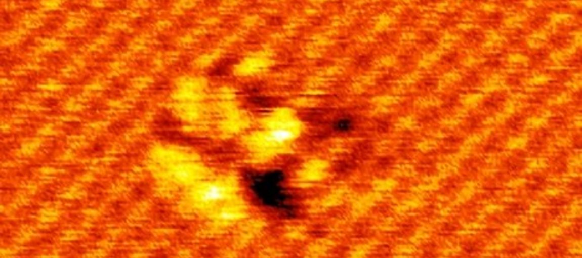
Nanodevices
Nanostructures have special electronic properties, high reactivity and many more. All of them are influenced strongly by the topography and size of the structure. To turn a Nanostructure into a nanodevice contacts and heterostructures have to be formed. Thus SPM and STS, LEEM and PEEM, as well, as (NAP)-XPS and ARPES are the key surface analytical methods, combined with deposition methods.
Your web browser is deprecated
This could effect the presentation and some functions of our website.
