Logo specsDetail

Multimethod System with XPS, LEEM and SPM

Linear Transfer System with XPS, LEEM and SPM for Wide Range of Modern Surface Science Applications

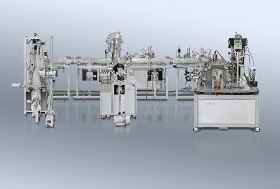
The SPECS Multimethod System with  LTS, XPS, LEEM and SPM is a fully equipped UHV analysis system for modern surface science applications. All systems are designed and manufactured at the SPECS headquarter in Berlin. A special engineering group personally accompanies the system process from the order placing until the final acceptance. Our engineers are dedicated to highest quality and usability of the system during design, testing and setup on site. Once the system is in full operation, a professional service team in our HQ and our worldwide branch offices takes care of a smooth and stable operation.

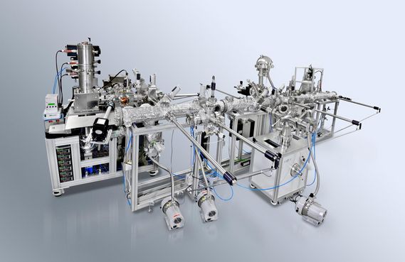
The SPECS linear transfer system (LTS) connects different satellite modules by a UHV vacuum tube with integrated sample carrier. Up to 5 slots for multiple samples can be moved automatically between the system interconnection points. The flexible design allows a cost efficient upgrade with additional transfer segments. Each segment can host up to two full scale satellite system modules. In this case, the LTS system comes with XPS, LEEM and SPM (Scanning Probe Microscopy) satellite chambers.

The LEEM  (Low Energy Electron Microscopy) system gives access to structural, chemical, electronic and magnetic properties of local dynamic surface processes. The SPM (Scanning Probe Microscopy) system allows local surface structure analysis with atomic resolution and local spectroscopy on atomic scale.

The typical vacuum in SPECS systems is better than 2 x 10⁻¹⁰ mbar achieved during assembly at SPECS. A final end pressure in the 10-11 mbar range is achievable. The standard pumping configuration consists of and ion getter pump (IGP), a titan sublimation pump (TSP) and a turbo molecular pump (TMP) with connecting to a roughing vacuum. Different pumping configurations are available on request including cryopumps, larger pumping schemes and also NEG pumps.

All systems are equipped with a rigid frame and included bake-out tents with automated heating systems. An electronics cabinet hosts all relevant electronics, a main power supply and a TCP/IP based communication platform for the control units.

All SPECS systems are ready for interconnections to other SPECS modules. Also the connection to existing systems can be tested on request.

KEY FEATURES

  • XPS analysis
  • Access to various structural, chemical, electronic and magnetic properties with LEEM
  • Atomic resolution real space analysis with SPM
  • Open and modular system design
  • Designed and tested in Berlin, Germany

MADE FOR THESE METHODS

3

PUBLICATIONS

  1. (2022) Advances in Analytical Instrumentation for Photoelectron Spectroscopy at Near-ambient Pressures

    Ever since the invention of photoelectron spectroscopy, researchers have attempted to analyze materials under conditions
    closely resembling their application environment. Near-Ambient Pressure X-ray Photoelectron Spectroscopy is a logical
    development in this quest, since it allows for analyzing non-vacuum compatible samples in general, and phase boundaries,
    such as solid|liquid or solid|gas interfaces, in particular. With the development of spectrometer systems compatible with
    analysis pressures of up to 100 mbar, many novel experimental geometries have been realized since the early 2000s. Since
    then, experimental capability and variety have further progressed through the proliferation of off-synchrotron laboratory
    systems, and advanced sample environments to simulate material usage conditions. This progress has, e.g., enabled the
    performance of operando spectroscopy during catalytic or electrochemical experiments. The present work gives, from an
    instrumental point of view, a short overview over basic system design considerations and recent developments in the field.


    M. Weidner and V. Streibel
    表面と真空 Vol. 65, No. 3, pp. 133–138, 2022
    Read more
  2. (2021) Stacking Relations and Substrate Interaction of Graphene on Copper Foil

    The crystallinity of graphene flakes and their orientation with respect to the Cu(111) substrate are investigated by means of low-energy electron microscopy (LEEM). The interplay between graphene and the metal substrate during chemical vapor deposition (CVD) introduces a restructuring of the metal surface into surface facets, which undergo a step bunching process during the growth of additional layers. Moreover, the surface facets introduce strain between the successively nucleated layers that follow the topography in a carpet-like fashion. The strain leads to dislocations in between domains of relaxed Bernal stacking. After the transfer onto an epitaxial buffer layer, the imprinted rippled structure of even monolayer graphene as well as the stacking dislocations are preserved. A similar behavior might also be expected for other CVD grown 2D materials such as hexagonal boron nitride or transition metal dichalcogenides, where stacking relations after transfer on a target substrate or heterostructure could become important in future experiments.


    P. Schädlich, F. Speck, C. Bouhafs, N. Mishra, S.Forti, C. Coletti, and T. Seyller
    Adv. Funct. Mater, Volume 8, Issue 7, April 9, 2021, 2002025
    Read more
  3. (2021) Spectroscopic analysis with tender X-rays: SpAnTeX, a new AP-HAXPES end-station at BESSY II

    We present a newly developed end-station at BESSY II dedicated to in situ Spectroscopic Analysis with Tender X-rays (SpAnTeX). The core of the end-station is a new SPECS PHOIBOS 150 HV NAP electron spectrometer. First, we show that the system has successfully achieved high electron transmission and detection efficiency under gas pressures up to 30 mbar and photon energies ranging between 200 eV and 10 keV. Second, using two features of this spectrometer (a new lateral resolution lens and a 3D delay line detector), we show that the endstation enables collection of the photoelectron spatial distribution under realistic working conditions (p ≥ 20 mbar) with a resolution better than 30 μm and the possibility to perform time resolved studies using a continuous tender X-ray source. We conclude by reporting an example of the possible experiments that can be performed using this new endstation using the Dip-and-Pull technique.

    Although mainly focused on the characterization of solid/liquid interfaces using AP-HAXPES, the end-station can be used at soft X-ray beamlines for more traditional AP-XPS experiments. The Dip-and-Pull module also demonstrates good electrochemical performance. The wide pressure and photon energy range covered by this end-station also enables investigations of solid/solid, solid/gas, liquid/vapor and liquid/liquid interfaces at pressures up to 30 mbar with tender X-rays.


    M. Favaro, P. C. J. Clark, M. J. Sear, M. Johansson, S. Maehl, R. van de Krol, and D.E. Starr
    Surface Science
    Volume 713, November 2021, 121903
    Read more
  4. (2020) Silicon Carbide Stacking-Order-Induced Doping Variation in Epitaxial Graphene

    Generally, it is supposed that the Fermi level in epitaxial graphene is controlled by two effects: p-type polarization doping induced by the bulk of the hexagonal silicon carbide (SiC)(0001) substrate and overcompensation by donor-like states related to the buffer layer. The presented work is evidence that this effect is also related to the specific underlying SiC terrace. Here a periodic sequence of non-identical SiC terraces is fabricated, which are unambiguously attributed to specific SiC surface terminations. A clear correlation between the SiC termination and the electronic graphene properties is experimentally observed and confirmed by various complementary surface-sensitive methods. This correlation is attributed to a proximity effect of the SiC termination-dependent polarization doping on the overlying graphene layer. These findings open a new approach for a nano-scale doping-engineering by the self-patterning of epitaxial graphene and other 2D layers on dielectric polar substrates.


    D. M. Pakdehi, P. Schädlich, T. T. N. Nguyen, A. A. Zakharov, S. Wundrack, E. Najafidehaghani, F. Speck, K. Pierz, T. Seyller, C. Tegenkamp, and H. W. Schumacher
    Adv. Funct. Mater, Volume 30, Issue 45, November 4, 2020, 2004695
    Read more
  5. (2020) In situ work-function measurement during chemical transformation of MoS2 to MoO3 by ambient-pressure x-ray photoelectron spectroscopy

    In this study, the oxidation of a two-dimensional (2D) MoS2 was performed as an alternative route
    for the synthesis of a 2D-layered MoO3 structure with high work function (WF) and hole mobility.
    The proposed method can also be used to tune the electronic properties (WF and bandgap) of MoO3/
    MoS2 composite-based semiconductors. By ambient pressure x-ray photoelectron spectroscopy
    (AP-XPS), in situ monitoring of the WF and chemical state of the surface was carried out during
    the oxidation of MoS2 to MoO3 layers. By heating the MoS2 sample in an O2 + Ar gas environment,
    the chemical transformation of the MoS2 to a MoO3/MoS2 composite layer and eventually to MoO3
    was observed. The chemically transformed MoO3 film had a properly layered structure, according
    to cross-sectional transmission electron microscopy and high-resolution grazing-incidence x-ray
    diffraction analyses. During the oxidation, the WF change according to the change in surface
    chemical state was simultaneously measured using Ar gas as a surface potential probe. This study
    demonstrates the capability of AP-XPS for the monitoring and optimization of the conditions for
    chemical transformation (oxidation) to achieve desired physical properties (e.g. WF).


    D. Lee, J. H. Jang, W.Song, J. Moon, Y. Kim, J. Lee,
    B. Jeong, and S. Park
    2D Mater. 7 (2020) 025014
    Read more
  6. (2020) AP-XPS beamline, a platform for operando science at Pohang Accelerator Laboratory

    Beamline 8A (BL 8A) is an undulator-based soft X-ray beamline at Pohang
    Accelerator Laboratory. This beamline is aimed at high-resolution ambientpressure
    X-ray photoelectron spectroscopy (AP-XPS), soft X-ray absorption
    spectroscopy (soft-XAS) and scanning photoemission microscopy (SPEM)
    experiments. BL 8A has two branches, 8A1 SPEM and 8A2 AP-XPS, that share
    a plane undulator, the first mirror (M1) and the monochromator. The photon
    beam is switched between the two branches by changing the refocusing mirrors
    after the monochromator. The acceptance angle of M1 is kept glancing at 1.2o,
    and Pt is coated onto the mirrors to achieve high reflectance, which ensures a
    wide photon energy range (100–2000 eV) with high resolution at a photon flux
    of ~1013 photons s-1. In this article, the main properties and performance of the
    beamline are reported, together with selected experiments performed on the
    new beamline and experimental system.


    G. Kim, Y. Yu, H. Lim, B.Jeong, J. Lee, J. Baik, B. S. Muna and K.-J. Kim
    J. Synchrotron Rad. (2020). 27, 507–514
    Read more
  7. (2020) Photoinduced Charge Carrier Dynamics and Electron Injection Efficiencies in Au Nanoparticle-Sensitized TiO2 Determined with Picosecond Time-Resolved X‑ray Photoelectron Spectroscopy

    Progress in the development of plasmon-enabled light-harvesting technologies requires a
    better understanding of their fundamental operating principles and current limitations. Here, we employ
    picosecond time-resolved X-ray photoemission spectroscopy to investigate photoinduced electron transfer in
    a plasmonic model system composed of 20 nm sized gold nanoparticles (NPs) attached to a nanoporous film
    of TiO2. The measurement provides direct, quantitative access to transient local charge distributions from
    the perspectives of the electron donor (AuNP) and the electron acceptor (TiO2). On average, approximately
    two electrons are injected per NP, corresponding to an electron injection yield per absorbed photon of 0.1%.
    Back electron transfer from the perspective of the electron donor is dominated by a fast recombination
    channel proceeding on a time scale of 60 ± 10 ps and a minor contribution that is completed after ∼1 ns.
    The findings provide a detailed picture of photoinduced charge carrier generation in this NP−semiconductor
    junction, with important implications for understanding achievable overall photon-to-charge conversion
    efficiencies.


    M. Borgwardt, J. Mahl, F.Roth, L. Wenthaus, F. Brauße, M.Blum,
    K. Schwarzburg, G. Liu, F.M. Toma, and O.Gessner
    The Journal of Physical Chemistry Letters. 2020, 11, 5476−5481
    Read more
  8. (2020) Identifying the Catalyst Chemical State and Adsorbed Species during Methanol Conversion on Copper Using Ambient Pressure X‐ray Spectroscopies

    Methanol is a promising chemical for the safe and efficient storage of hydrogen, where methanol conversion reactions can
    generate a hydrogen‐containing gas mixture. Understanding the chemical state of the catalyst over which these reactions
    occur and the interplay with the adsorbed species present is key to the design of improved catalysts and process conditions.
    Here we study polycrystalline Cu foils using ambient pressure X‐ray spectroscopies to reveal the Cu oxidation state and
    identify the adsorbed species during partial oxidation (CH3OH + O2), steam reforming (CH3OH + H2O), and autothermal
    reforming (CH3OH + O2 + H2O) of methanol at 200 °C surface temperature and in the mbar pressure range. We find that the
    Cu surface remains highly metallic throughout partial oxidation and steam reforming reactions, even for oxygen‐rich
    conditions. However, for autothermal reforming the Cu surface shows significant oxidation towards Cu2O. We rationalise
    this behaviour on the basis of the shift in equilibrium of the CH3OH* + O* ⇌ CH3O* + OH* caused by the addition of H2O.


    B. Eren, C. G. Sole, J. S. Lacasa, D. Grinter, F. Venturini, G. Held,
    C. S. Esconjauregui, and R. S. Weatherup
    Physical Chemistry Chemical Physics, 2020, 00, 1‐8
    Read more
  9. (2019) Ionic-Activated Chemiresistive Gas Sensors for Room-Temperature Operation

    The development of high performance gas sensors that operate at room temperature
    has attracted considerable attention. Unfortunately, the conventional
    mechanism of chemiresistive sensors is restricted at room temperature by
    insufficient reaction energy with target molecules. Herein, novel strategy for
    room temperature gas sensors is reported using an ionic-activated sensing
    mechanism. The investigation reveals that a hydroxide layer is developed by
    the applied voltages on the SnO2 surface in the presence of humidity, leading
    to increased electrical conductivity. Surprisingly, the experimental results
    indicate ideal sensing behavior at room temperature for NO2 detection with
    sub-parts-per-trillion (132.3 ppt) detection and fast recovery (25.7 s) to 5 ppm
    NO2 under humid conditions. The ionic-activated sensing mechanism is
    proposed as a cascade process involving the formation of ionic conduction,
    reaction with a target gas, and demonstrates the novelty of the approach. It
    is believed that the results presented will open new pathways as a promising
    method for room temperature gas sensors.


    Y. G. Song, Y.-S. Shim, J. M. Suh, M.-S. Noh, G. S. Kim,
    K. S. Choi, B. Jeong, S. Kim, H. W. Jang, B.-K. Ju,
    and C.-Y. Kang
    Small 2019, 15, 1902065
    Read more
  10. (2019) Propane dehydrogenation over vanadium-doped zirconium oxide catalysts

    Bulk ZrO2 is a highly active and selective catalyst for dehydrogenation of propane (PDH), in which coordinatively
    unsaturated Zr cations (Zrcus4+) serve as active sites. Substitution of dopant ions into Zr lattice can improve its catalytic activity by generating more Zrcus4+ sites. In this work, a series of vanadium-doped ZrO2 metal oxides (VZrO-x) have been prepared and the influences of vanadium content on their properties have been systematically investigated. Various characterization techniques showed that an appropriate amount of vanadium dopant helps more Zrcus4+ sites to be created by a structural transformation and H2 pretreatment. However, excess vanadium dopant led to a negative effect on the catalytic activity owing to the formation of
    bulk-like V2O5 crystallites. The catalytic activity of VZrO-x is well correlated with the amount of Lewis acid sites
    because Zrcus4+ cations correspond to Lewis acid sites. The VZrO-8 catalyst exhibited two times higher activity
    than pure ZrO2. Moreover, for repeated cycles the activity was totally recovered by oxidative regeneration
    followed by reductive pretreatment. Finally, the performance test results showed that H2 co-feeding can further
    enhance the activity by suppressing coke deposition during PDH.


    N. Jeon, H. Choe, B.Jeong, and Y. Yun
    Catalysis Today
    Read more
  11. (2019) Cu-promoted zirconia catalysts for non-oxidative propane dehydrogenation

    Bulk ZrO2 has shown high activity and selectivity for propane dehydrogenation (PDH). Its catalytic performance
    can be enhanced by substitution of the Zr ions with suitable dopant ions. In this study, a series of Cu-doped ZrO2
    metal oxides (CuZrO-x) have been prepared using the co-precipitation method and the effects of the amount of
    dopant on their properties have been investigated. The appropriate amount of Cu dopant promotes the creation
    of oxygen vacancies and coordinatively unsaturated Zrcus4+ sites, active sites for PDH; however, excess Cu forms
    bulk CuO in the CuZrO-x catalysts resulting in decreased activity. The catalytic activity for PDH is closely
    correlated to the amount of weak Lewis acid sites in CuZrO-x. Moreover, a comparison of the CuZrO-x properties
    with those of Cu-impregnated ZrO2 has shown that the amount of acid sites and therefore, the catalytic performance,
    depends on the doping method.


    N. Jeon, H. Choe, B.Jeong, and Y. Yun
    Applied Catalysis A, General 586 (2019) 117211
    Read more
  12. (2019) Efficient charge generation from triplet excitons in metal-organic heterojunctions

    The success of many emerging molecular electronics concepts hinges on an atomistic understanding of
    the underlying electronic dynamics. We employ picosecond time-resolved x-ray photoemission spectroscopy
    (tr-XPS) to elucidate the roles of singlet and triplet excitons for photoinduced charge generation at a copperphthalocyanine–
    C60 heterojunction. Contrary to common belief, fast intersystem crossing to triplet excitons
    after photoexcitation is not a loss channel but contributes to a significantly larger extent to the time-integrated
    interfacial charge generation than the initially excited singlet excitons. The tr-XPS data provide direct access to
    the diffusivity of the triplet excitons DCuPc = (1.8 ± 1.2) × 10−5 cm2/s (where CuPc is copper-phthalocyanine)
    and their diffusion length Ldiff = (8 ± 3) nm.


    F. Roth, S.Neppl, A. Shavorskiy, T. Arion, J.Mahl, H. O. Seo,
    H. Bluhm, Z.Hussain, O. Gessner, and W. Eberhardt.
    PHYSICAL REVIEW B 99, 020303(R) (2019)
    Read more
  13. (2015) Low-Energy Electron Potentiometry: Contactless Imaging of Charge Transport on the Nanoscale

    Charge transport measurements form an essential tool in condensed matter physics. The usual approach is to contact a sample by two or four probes, measure the resistance and derive the resistivity, assuming homogeneity within the sample. A more thorough understanding, however, requires knowledge of local resistivity variations. Spatially resolved information is particularly important when studying novel materials like topological insulators, where the current is localized at the edges, or quasi-two-dimensional (2D) systems, where small-scale variations can determine global properties. Here, we demonstrate a new method to determine spatially-resolved voltage maps of current-carrying samples. This technique is based on low-energy electron microscopy (LEEM) and is therefore quick and non-invasive. It makes use of resonance-induced contrast, which strongly depends on the local potential. We demonstrate our method using single to triple layer graphene. However, it is straightforwardly extendable to other quasi-2D systems, most prominently to the upcoming class of layered van der Waals materials.


    J. Kautz, J. Jobst, C. Sorger, R. M. Tromp, H. B. Weber und S. J. van der Molen
    Scientific Reports volume 5, Article number: 13604 (2015)
    Read more
  14. (2015) Time-resolved X-ray photoelectron spectroscopy techniques for thestudy of interfacial charge dynamics

    X-ray photoelectron spectroscopy (XPS) is one of the most powerful techniques to quantitatively ana-lyze the chemical composition and electronic structure of surfaces and interfaces in a non-destructivefashion. Extending this technique into the time domain has the exciting potential to shed new lighton electronic and chemical dynamics at surfaces by revealing transient charge configurations withelement- and site-specificity. Here, we describe prospects and challenges that are associated with theimplementation of picosecond and femtosecond time-resolved X-ray photoelectron spectroscopy atthird-generation synchrotrons and X-ray free-electron lasers, respectively. In particular, we discuss aseries of laser-pump/X-ray-probe photoemission experiments performed on semiconductor surfaces,molecule-semiconductor interfaces, and films of semiconductor nanoparticles that demonstrate the highsensitivity of time-resolved XPS to light-induced charge carrier generation, diffusion and recombinationwithin the space charge layers of these materials. Employing the showcase example of photo-inducedelectronic dynamics in a dye-sensitized semiconductor system, we highlight the unique possibility toprobe heterogeneous charge transfer dynamics from both sides of an interface, i.e., from the perspectiveof the molecular electron donor and the semiconductor acceptor, simultaneously. Such capabilities willbe crucial to improve our microscopic understanding of interfacial charge redistribution and associatedchemical dynamics, which are at the heart of emerging energy conversion, solar fuel generation, andenergy storage technologies.


    S. Neppl, O. Gessner
    Journal of Electron Spectroscopy and Related Phenomena 200 (2015) 64–77
    Read more
  15. (2014) Sub-nanosecond time-resolved ambient-pressure X-ray photoelectron spectroscopy setup for pulsed and constant wave X-ray light sources

    An apparatus for sub-nanosecond time-resolved ambient-pressure X-ray photoelectron spectroscopy
    studies with pulsed and constant wave X-ray light sources is presented. A differentially pumped
    hemispherical electron analyzer is equipped with a delay-line detector that simultaneously records
    the position and arrival time of every single electron at the exit aperture of the hemisphere with
    ∼0.1 mm spatial resolution and ∼150 ps temporal accuracy. The kinetic energies of the photoelectrons
    are encoded in the hit positions along the dispersive axis of the two-dimensional detector. Pumpprobe
    time-delays are provided by the electron arrival times relative to the pump pulse timing. An
    average time-resolution of (780 ± 20) ps (FWHM) is demonstrated for a hemisphere pass energy Ep
    = 150 eV and an electron kinetic energy range KE = 503–508 eV. The time-resolution of the setup
    is limited by the electron time-of-flight (TOF) spread related to the electron trajectory distribution
    within the analyzer hemisphere and within the electrostatic lens system that images the interaction
    volume onto the hemisphere entrance slit. The TOF spread for electrons with KE = 430 eV varies
    between ∼9 ns at a pass energy of 50 eV and ∼1 ns at pass energies between 200 eV and 400 eV. The
    correlation between the retarding ratio and the TOF spread is evaluated by means of both analytical
    descriptions of the electron trajectories within the analyzer hemisphere and computer simulations of
    the entire trajectories including the electrostatic lens system. In agreement with previous studies, we
    find that the by far dominant contribution to the TOF spread is acquired within the hemisphere. However,
    both experiment and computer simulations show that the lens system indirectly affects the time
    resolution of the setup to a significant extent by inducing a strong dependence of the angular spread
    of electron trajectories entering the hemisphere on the retarding ratio. The scaling of the angular
    spread with the retarding ratio can be well approximated by applying Liouville’s theorem of constant
    emittance to the electron trajectories inside the lens system. The performance of the setup is demonstrated
    by characterizing the laser fluence-dependent transient surface photovoltage response of a
    laser-excited Si(100) sample. © 2014 AIP Publishing LLC.


    A. Shavorskiy, S. Neppl, D. S. Slaughter, J. P. Cryan, K. R. Siefermann, F. Weise,
    Mf Lin, C. Bacellar, M. P. Ziemkiewicz, I. Zegkinoglou, M. W. Fraund, C.
    Khurmi, M. P. Hertlein, T. W. Wright, N. Huse, R. W. Schoenlein, T. Tyliszczak, G.
    Coslovich, J.
    AIP Review of Scientific Instruments 85, 093102 (2014)
    Read more
  16. (2014) Atomic-Scale Perspective of Ultrafast Charge Transfer at a Dye−Semiconductor Interface

    Understanding interfacial charge-transfer processes on the atomic level is
    crucial to support the rational design of energy-challenge relevant systems such as solar cells,
    batteries, and photocatalysts. A femtosecond time-resolved core-level photoelectron spectroscopy
    study is performed that probes the electronic structure of the interface between
    ruthenium-based N3 dye molecules and ZnO nanocrystals within the first picosecond after
    photoexcitation and from the unique perspective of the Ru reporter atom at the center of the
    dye. A transient chemical shift of the Ru 3d inner-shell photolines by (2.3 ± 0.2) eV to higher
    binding energies is observed 500 fs after photoexcitation of the dye. The experimental results
    are interpreted with the aid of ab initio calculations using constrained density functional
    theory. Strong indications for the formation of an interfacial charge-transfer state are presented,
    providing direct insight into a transient electronic configuration that may limit the
    efficiency of photoinduced free charge-carrier generation.


    K.R. Siefermann, C. D. Pemmaraju, S. Neppl, A. Shavorskiy,
    A. A. Cordones, J. Vura-Weis, D. S. Slaughter, F. P. Sturm, F. Weise,
    H. Bluhm, M. L. Strader, H. Cho, MF Lin, C. Bacellar,
    C. Khurmi, J. Guo, G. Coslovich, J. S. Robinson, R. A. Kaindl,
    R. W.
    The Journal of Physical Chemistry Letters. 2014, 5, 2753−2759
    Read more
Close
Your web browser is deprecated
This could effect the presentation and some functions of our website.