Logo specs-groupDetail

LEEM/PEEM

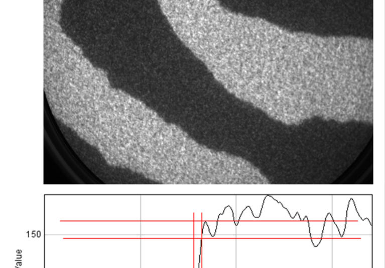
The SPECS LEEM instrument FE-LEEM P90 is a next generation Low Energy Electron Microscope with unsurpassed 5 nm resolution for dynamic LEEM microscopy experiments. With this instrument, based on the design of Dr. Rudolf Tromp, nanometer scale processes on surfaces can be observed in real-time. The instrument is always equipped with an energy filter for spectromicroscopy and is available in a standard version, an aberration corrected version for lateral LEEM resolutions below 2 nm and as a Near Ambient Pressure version for studies in pressures up to 1 mbar.

Electron Microscope LEEM/PEEM with model number FE-LEEM P90

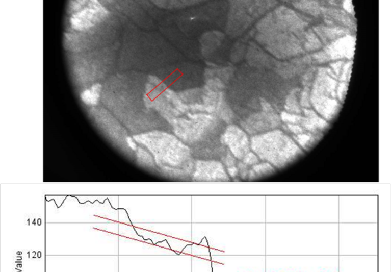
FE-LEEM/PEEM P90 forms a state-of-the-art surface electron microscope reaching highest resolution in an easy-to-use compact design. Key features are fast specimen exchange, low vibration measurements, and in situ studies on dynamic surface processes. The base system is the PEEM P90 (without electron source) or the FE-LEEM P90 (equipped with a cold field emission electron source). Both are turnkey multichamber systems with an energy filter, sample storage and all necessary vacuum equipment. The system can also be upgraded with an optional aberration corrector for improved transmission and resolution. The FE-LEEM/PEEM is also available in a near ambient pressure version enabling operando studies under pressure conditions of up to 1 mbar.

RELATED PRODUCTS

APPLICATION NOTES

PUBLICATIONS

  1. (2021) In situ identification of the metallic state of Ag nanoclusters in oxidative dispersion

    Oxidative dispersion has been widely used in regeneration of sintered metal catalysts and fabrication of single atom catalysts, which is attributed to an oxidation-induced dispersion mechanism. However, the interplay of gas-metal-support interaction in the dispersion processes, especially the gas-metal interaction has not been well illustrated. Here, we show dynamic dispersion of silver nanostructures on silicon nitride surface under reducing/oxidizing conditions and during carbon monoxide oxidation reaction. Utilizing environmental scanning (transmission) electron microscopy and near-ambient pressure photoelectron spectroscopy/photoemission electron microscopy, we unravel a new adsorption-induced dispersion mechanism in such a typical oxidative dispersion process. The strong gas-metal interaction achieved by chemisorption of oxygen on nearly-metallic silver nanoclusters is the internal driving force for dispersion. In situ observations show that the dispersed nearly-metallic silver nanoclusters are oxidized upon cooling in oxygen atmosphere, which could mislead to the understanding of oxidation-induced dispersion. We further understand the oxidative dispersion mechanism from the view of dynamic equilibrium taking temperature and gas pressure into account, which should be applied to many other metals such as gold, copper, palladium, etc. and other reaction conditions.


    Rongtan Li, Xiaoyan Xu, Beien Zhu, Xiao-Yan Li, Yanxiao Ning, Rentao Mu, Pengfei Du, Mengwei Li, Huike Wang, Jiajie Liang, Yongsheng Chen, Yi Gao, Bing Yang, Qiang Fu & Xinhe Bao
    NATURE COMMUNICATIONS | (2021) 12:1406
    Read more
  2. (2021) Stacking Relations and Substrate Interaction of Graphene on Copper Foil

    The crystallinity of graphene flakes and their orientation with respect to the Cu(111) substrate are investigated by means of low-energy electron microscopy (LEEM). The interplay between graphene and the metal substrate during chemical vapor deposition (CVD) introduces a restructuring of the metal surface into surface facets, which undergo a step bunching process during the growth of additional layers. Moreover, the surface facets introduce strain between the successively nucleated layers that follow the topography in a carpet-like fashion. The strain leads to dislocations in between domains of relaxed Bernal stacking. After the transfer onto an epitaxial buffer layer, the imprinted rippled structure of even monolayer graphene as well as the stacking dislocations are preserved. A similar behavior might also be expected for other CVD grown 2D materials such as hexagonal boron nitride or transition metal dichalcogenides, where stacking relations after transfer on a target substrate or heterostructure could become important in future experiments.


    P. Schädlich, F. Speck, C. Bouhafs, N. Mishra, S.Forti, C. Coletti, and T. Seyller
    Adv. Funct. Mater, Volume 8, Issue 7, April 9, 2021, 2002025
    Read more
  3. (2020) Silicon Carbide Stacking-Order-Induced Doping Variation in Epitaxial Graphene

    Generally, it is supposed that the Fermi level in epitaxial graphene is controlled by two effects: p-type polarization doping induced by the bulk of the hexagonal silicon carbide (SiC)(0001) substrate and overcompensation by donor-like states related to the buffer layer. The presented work is evidence that this effect is also related to the specific underlying SiC terrace. Here a periodic sequence of non-identical SiC terraces is fabricated, which are unambiguously attributed to specific SiC surface terminations. A clear correlation between the SiC termination and the electronic graphene properties is experimentally observed and confirmed by various complementary surface-sensitive methods. This correlation is attributed to a proximity effect of the SiC termination-dependent polarization doping on the overlying graphene layer. These findings open a new approach for a nano-scale doping-engineering by the self-patterning of epitaxial graphene and other 2D layers on dielectric polar substrates.


    D. M. Pakdehi, P. Schädlich, T. T. N. Nguyen, A. A. Zakharov, S. Wundrack, E. Najafidehaghani, F. Speck, K. Pierz, T. Seyller, C. Tegenkamp, and H. W. Schumacher
    Adv. Funct. Mater, Volume 30, Issue 45, November 4, 2020, 2004695
    Read more
  4. (2015) Low-Energy Electron Potentiometry: Contactless Imaging of Charge Transport on the Nanoscale

    Charge transport measurements form an essential tool in condensed matter physics. The usual approach is to contact a sample by two or four probes, measure the resistance and derive the resistivity, assuming homogeneity within the sample. A more thorough understanding, however, requires knowledge of local resistivity variations. Spatially resolved information is particularly important when studying novel materials like topological insulators, where the current is localized at the edges, or quasi-two-dimensional (2D) systems, where small-scale variations can determine global properties. Here, we demonstrate a new method to determine spatially-resolved voltage maps of current-carrying samples. This technique is based on low-energy electron microscopy (LEEM) and is therefore quick and non-invasive. It makes use of resonance-induced contrast, which strongly depends on the local potential. We demonstrate our method using single to triple layer graphene. However, it is straightforwardly extendable to other quasi-2D systems, most prominently to the upcoming class of layered van der Waals materials.


    J. Kautz, J. Jobst, C. Sorger, R. M. Tromp, H. B. Weber und S. J. van der Molen
    Scientific Reports volume 5, Article number: 13604 (2015)
    Read more
  5. (2014) Buffer layer free graphene on SiC(0001) via interface oxidation in water vapor

    Intercalation of various elements has become a popular technique to decouple the buffer layer of epitaxial graphene on SiC(0 0 0 1) from the substrate. Among many other elements, oxygen can be used to passivate the SiC interface, causing the buffer layer to transform into graphene. Here, we study a gentle oxidation of the interface by annealing buffer layer and monolayer graphene samples in water vapor. X-ray photoelectron spectroscopy demonstrates the decoupling of the buffer layer from the SiC substrate. Raman spectroscopy is utilized to investigate a possible introduction of defects. Angle-resolved photoemission spectroscopy shows that the electronic structure of the water vapor treated samples. Low-energy electron microscopy (LEEM) measurements demonstrate that the decoupling takes place without changes in the surface morphology. The LEEM reflectivity spectra are discussed in terms of two different interpretations.


    M. Ostler, F. Fromm, R.J. Koch, P. Wehrfritz, F. Speck, H. Vita, S. Böttcher, K. Horn, T. Seyller
    Carbon 70, pp. 258-265
    Read more
  6. (2013) Direct growth of quasi-free-standing epitaxial graphene on nonpolar SiC surfaces

    During the graphitization of polar SiC(0001) surfaces through thermal decomposition, a strongly bound carbon-rich layer forms at the graphene/SiC interface. This layer is responsible for the system's high electron-doping and contributes to the degradation of the electrical properties of the overlying graphene. In this study, with the aid of photoelectron spectroscopy, low-energy electron microscopy, low-energy electron diffraction, and the density functional theory, we show that if the graphitization process starts from the nonpolar (11¯20) and (1¯100) surfaces instead, no buffer layer is formed. We correlate this direct growth of quasi-free-standing graphene over the substrate with the inhibited formation of tetrahedral bonds between the nonpolar surface and the carbon monolayer.


    M. Ostler, I. Deretzis, S. Mammadov, F. Giannazzo, G. Nicotra, C. Spinella, Th. Seyller, A. La Magna
    Phys. Rev. B 88, 085408
    Read more
  7. (2017) Growth and Intercalation of Graphene on Silicon Carbide Studied by Low‐Energy Electron Microscopy

    Based on its electronic, structural, chemical, and mechanical properties, many potential applications have been proposed for graphene. In order to realize these visions, graphene has to be synthesized, grown, or exfoliated with properties that are determined by the targeted application. Growth of so‐called epitaxial graphene on silicon carbide by sublimation of silicon in an argon atmosphere is one particular method that could potentially lead to electronic applications. In this contribution we summarize our recent work on different aspects of epitaxial graphene growth and interface manipulation by intercalation, which was performed by a combination of low‐energy electron microscopy, low‐energy electron diffraction, atomic force microscopy and photoelectron spectroscopy.


    F. Speck, M. Ostler, S. Besendörfer, J. Krone, M. Wanke, T. Seyller
    Annalen der Physik, 529 (11), 1700046
    Read more
  8. (2014) Healing of graphene on single crystalline Ni(111) films

    The annealing of graphene layers grown on 150 nm thick single crystal Ni(111) films was investigated in situ by low energy electron microscopy and photoemission electron microscopy. After growth, by means of chemical vapor deposition of ethylene, the graphene layers consist of several domains showing different orientations with respect to the underlying Ni surface and also of small bilayer areas. It is shown that, in a controlled process, the rotated domains can be transformed into lattice-aligned graphene, and the bilayer areas can be selectively dissolved, so that exclusively the aligned monolayer graphene is obtained. The ordering mechanism involves transport of C atoms across the surface and solution in the bulk.


    P. Zeller, F. Speck, M. Weinl, M. Ostler, M. Schreck, T. Seyller, J. Wintterlin
    Appl. Phys. Lett. 105, 191612
    Read more
  9. (2017) Single Crystalline Metal Films as Substrates for Graphene Growth

    Single crystalline metal films deposited on YSZ‐buffered Si(111) wafers were investigated with respect to their suitability as substrates for epitaxial graphene. Graphene was grown by CVD of ethylene on Ru(0001), Ir(111), and Ni(111) films in UHV. For analysis a variety of surface science methods were used. By an initial annealing step the surface quality of the films was strongly improved. The temperature treatments of the metal films caused a pattern of slip lines, formed by thermal stress in the films, which, however, did not affect the graphene quality and even prevented wrinkle formation. Graphene was successfully grown on all three types of metal films in a quality comparable to graphene grown on bulk single crystals of the same metals. In the case of the Ni(111) films the originally obtained domain structure of rotational graphene phases could be transformed into a single domain by annealing. This healing process is based on the control of the equilibrium between graphene and dissolved carbon in the film. For the system graphene/Ni(111) the metal, after graphene growth, could be removed from underneath the epitaxial graphene layer by a pure gas phase reaction, using the reaction of CO with Ni to give gaseous Ni(CO)4.


    P. Zeller, M. Weinl, F. Speck, M. Ostler, A.-K. Henß, T. Seyller, M. Schreck, J. Wintterlin
    Annalen der Physik, 529 (11), 1700023
    Read more
Close
Your web browser is deprecated
This could effect the presentation and some functions of our website.