Logo nanonis

Tramea

The Nanonis Tramea™ base configuration provides all elements required for performing high-speed DC transport measurements: 8 precision, high-speed DC sources, 8 precision analog inputs, and a full-featured software solution for data generation and acquisition. All signal conditioning, FPGA and real-time signal processing are also included in the base configuration, which offers a complete framework that can be adapted and extended with a wide range of add-on modules

Base configuration: Real-time Controller, Signal Conversion unit and Nanonis software.

RELATED PRODUCTS

APPLICATION NOTES

Probing Quantum Transport by Scanning Gate Microscopy (SGM)
Most scanning probe microscopy techniques are ideal to investigate theproperties of the first few atomic layers of a surface, but are useless when the system of interest is buried deeper.…
download PDF
Topological Insulator Josephson junctions
In a topological insulator (TI), the electronic structure of the bulk reveals a unique topology that leads to the formation of conducting surface states with intriguing properties. The…
download PDF
Measuring Electron Temperature using Nanonis Tramea
The Nanonis Tramea Quantum Transport Measurement System (QTMS) was used to measure electron transport through an electrostatically defined Gallium Arsenide (GaAs) quantum dot in an Oxford…
download PDF
Characterization of Germanium Nanowire
Using a combination of the Nanonis Tramea quantum transport measurement system fully integrated with an Oxford Instruments HelioxVL refrigerator, the energy levels of a qubit have been…
download PDF
Transport and RF-Reflectometry Measurements of CMOS Nanodevices
Pioneering work on semiconductor quantum dots has shown that quantum dots are promising candidates as a building block (qubit) for quantum information and computation. Quantum dots are…
download PDF
Tuning and Operation of Quantum Dots and Related Apparatus
Spin qubits in quantum dots are promising candidates towards quantum computation. However, a considerable amount of technical development is still necessary before the advent of a quantum…
download PDF
Physics on the Level of Single Electrons
When shrinking the size of physical systems, it often becomes unclear in which way the physical laws are still valid. For example, thermodynamics is a phenom-enological theory which relies…
download PDF

PUBLICATIONS

  1. (2021) Gate-Defined Quantum Confinement in CVD 2D WS2

    Temperature-dependent transport measurements are performed on the same
    set of chemical vapor deposition (CVD)-grown WS2 single- and bilayer devices
    before and after atomic layer deposition (ALD) of HfO2. This isolates the influence
    of HfO2 deposition on low-temperature carrier transport and shows that
    carrier mobility is not charge impurity limited as commonly thought, but due
    to another important but commonly overlooked factor: interface roughness.
    This finding is corroborated by circular dichroic photoluminescence spectroscopy,
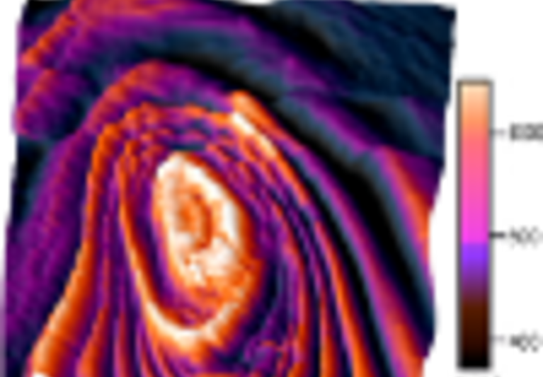
    X-ray photoemission spectroscopy, cross-sectional scanning transmission
    electron microscopy, carrier-transport modeling, and density functional
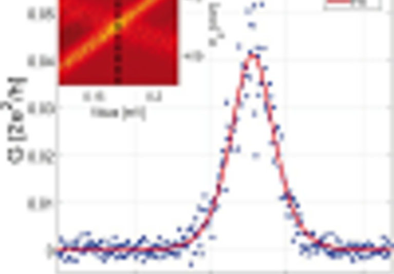
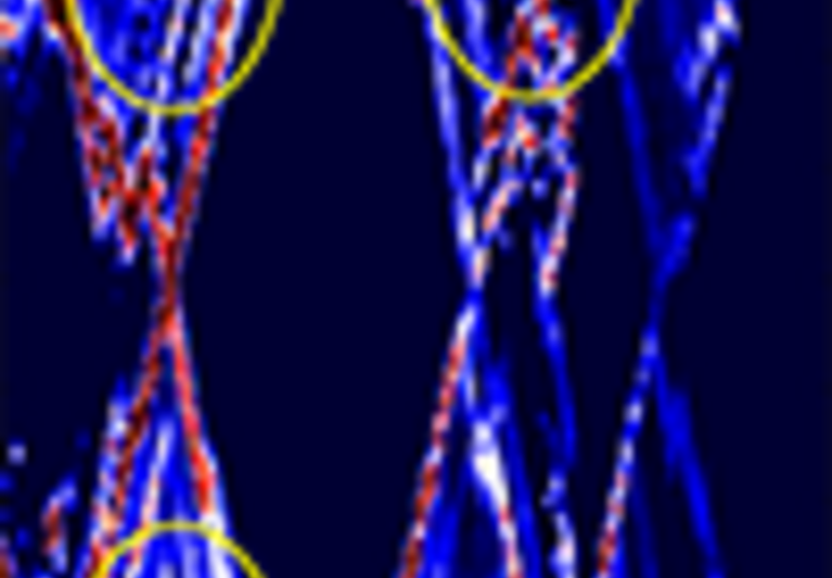
    modeling. Finally, electrostatic gate-defined quantum confinement is demonstrated
    using a scalable approach of large-area CVD-grown bilayer WS2
    and ALD-grown HfO2. The high dielectric constant and low leakage current
    enabled by HfO2 allows an estimated quantum dot size as small as 58 nm.
    The ability to lithographically define increasingly smaller devices is especially
    important for transition metal dichalcogenides due to their large effective
    masses, and should pave the way toward their use in quantum information
    processing applications.


    C. S. Lau, J. Y. Chee, Z.-E. Ooi, S. W. Tong, M. Bosman, F. Bussolotti,
    T. Wang, S. L. Teo, C. P. Y. Wong, J. W. Chai, Z. M. Zhang, K.-W. Ang, and
    K. E. J. Goh
    Adv. Mater. 2021, 2103907
    Read more
  2. (2021) Quantum confinement of the Dirac surface states in topological-insulator nanowires

    The non-trivial topology of three-dimensional topological insulators dictates the appearance of gapless Dirac surface states. Intriguingly, when made into a nanowire, quantum confinement leads to a peculiar gapped Dirac sub-band structure. This gap is useful for, e.g., future Majorana qubits based on TIs. Furthermore, these sub-bands can be manipulated by a magnetic flux and are an ideal platform for generating stable Majorana zero modes, playing a key role in topological quantum computing. However, direct evidence for the Dirac sub-bands in TI nanowires has not been reported so far. Here, using devices fabricated from thin bulk-insulating (Bi1−xSbx)2Te3 nanowires we show that non-equidistant resistance peaks, observed upon gate-tuning the chemical potential across the Dirac point, are the unique signatures of the quantized sub-bands. These TI nanowires open the way to address the topological mesoscopic physics, and eventually the Majorana physics when proximitized by an s-wave superconductor.


    F. Münning, O. Breunig, H. F. Legg, S. Roitsch, D. Fan, M. Rößler, A. Rosch, and Y. Ando
    Nat Commun 12, 1038 (2021)
    Read more
  3. (2019) Gate Tunable Hole Charge Qubit Formed in a Ge/Si Nanowire Double Quantum Dot Coupled to Microwave Photons

    A controllable and coherent light-matter interface is an essential element for a scalable quantum information processor. Strong coupling to an on-chip cavity has been accomplished in various electron quantum dot systems, but rarely explored in the hole systems. Here we demonstrate a hybrid architecture comprising a microwave transmission line resonator controllably coupled to a hole charge qubit formed in a Ge/Si core/shell nanowire (NW), which is a natural one-dimensional hole gas with a strong spin–orbit interaction (SOI) and lack of nuclear spin scattering, potentially enabling fast spin manipulation by electric manners and long coherence times. The charge qubit is established in a double quantum dot defined by local electrical gates. Qubit transition energy can be independently tuned by the electrochemical potential difference and the tunnel coupling between the adjacent dots, opening transverse (σx) and longitudinal (σz) degrees of freedom for qubit operation and interaction. As the qubit energy is swept across the photon level, the coupling with resonator is thus switched on and off, as detected by resonator transmission spectroscopy. The observed resonance dynamics is replicated by a complete quantum numerical simulation considering an efficient charge dipole-photon coupling with a strength up to 2π × 55 MHz, yielding an estimation of the spin-resonator coupling rate through SOI to be about 10 MHz. The results inspire the future researches on the coherent hole-photon interaction in Ge/Si nanowires.


    R. Wang, R. S. Deacon, J. Sun, J. Yao, C. M. Lieber and K. Ishibashi
    Nano Lett. 2019, 19, 2, 1052-1060
    Read more
Close
Your web browser is deprecated
This could effect the presentation and some functions of our website.